Resources

Showing 121-130 of 180
  • Media Image
    Paolo Longo, Ph.D., Gatan, Inc. Sample courtesy of Dr. P. Rice and Dr. T. Topuria at IBM (Almaden), San Jose, CA Microscope courtesy of Dr. P. Rice and Dr. T. Topuria at IBM (Almaden), San Jose, CA Acknowledgements to Dr. P. Rice and Dr. T. Topuria at IBM (Almaden), San Jose, CA for helping set up microscope for experiment.

    Methods

  • Media Image
    Paolo Longo, Ph.D., Gatan, Inc. Sample courtesy of by Dr. P. Rice and Dr. T. Topuria at IBM (Almaden), San Jose CA Microscope courtesy of Dr. P. Rice and Dr. T. Topuria at IBM (Almaden), San Jose CA Acknowledgements to Dr. P. Rice and Dr. T. Topuria at IBM (Almaden), San Jose, CA for helping set up microscope for experiment.

    Methods

  • Media Image
    Paolo Longo, Ph.D., Gatan, Inc. Sample courtesy of Dr. P. Rice and Dr. T. Topuria at IBM (Almaden), San Jose, CA Microscope courtesy of Dr. P. Rice and Dr. T. Topuria at IBM (Almaden), San Jose, CA Acknowledgement to Dr. P. Rice and Dr. T. Topuria at IBM (Almaden) for helping set up microscope for experiment.

    Legend

    Green: Ti L at 456 eV; red: Sr L at 1940 eV; purple: La M at 832 eV; blue: Mn L at 640 eV

    Methods

  • Media Image
    Paolo Longo PhD, Gatan, Inc. Sample courtesy of Professor Robert Wallace at UTD, Richardson, TX Microscope courtesy of Professor Ray Carpenter, Arizona State University, Tempe AZ Acknowledgement to Dr. Toshiro Aoki at Jeol USA (now at ASU) for helping set up microscope for experiment.

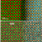
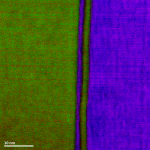
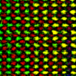
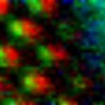
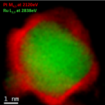
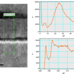
    InP substrate is very beam sensitive; EELS analysis was carried out at high-speed to avoid electron beam-induced damage.

    Methods

    Probe-corrected Jeol ARM 200 TEM/STEM microscope; S-FEG emission gun; Enfinium™ ER system; voltage: 200 kV; STEM mode

  • Media Image
    Paolo Longo, Ph.D., Gatan, Inc. Sample courtesy of Professor David J. Smith at Arizona State University, Tempe, AZ Microscope courtesy of Professor Ray Carpenter at Arizona State University, Tempe, AZ Acknowledgement to Dr. Toshiro Aoki at Jeol USA (now at ASU) for helping set up microscope for experiment.

    Legend

    Red: Ti L at 456 eV; green: Sr L at 1940 eV; yellow: La M at 832 eV; blue: Mn L at 640 eV

    Methods

  • Media Image
    Paolo Longo, Ph.D., Gatan, Inc. Sample courtesy of University of Glasgow Microscopecourtesy of Professor Gerald Kothleitner, TU-Graz, Austria

    Methods

  • Media Image
    Paolo Longo, Ph.D., Gatan, Inc. Sample courtesy of University of Glasgow Microscope courtesy of Dr. Yan Xin at Florida State University, Tallahassee, FL Acknowledgement to Dr. Toshiro Aoki at Jeol USA (now at ASU) for helping set up microscope for experiment.

    Dumbbell structure of GaAs on left hand side of color map is clearly resolved, and Ga and As atomic columns are visible. Interface region shows presence of Ga2O monolayer responsible for keeping Fermi level unpinned, which allows the electronic device to be turned on or off.

  • Media Image
    Paolo Longo, Ph.D., Gatan, Inc. Sample courtesy of Professor Gianluigi Botton at CCEM, Hamilton, ON, Canada Microscope courtesy of CCEM, Hamilton ON, Canada Acknowledgement to Dr. Andreas Korinek at CCEM for helping set up microscope for experiment.

    Methods

  • Media Image
    Paolo Longo, Ph.D., Gatan, Inc. Sample courtesy of Dr. Giuseppe Nicotra at IMM-CNR, Catania, Italy Microscope courtesy of IMM-CNR, Catania, Italy

    Methods

    Probe-corrected ARM 200F TEM/STEM microscope; C-FEG emission gun; GIF Quantum® ER system; voltage: 60 kV; STEM mode; EELS low-loss spectrum (0 – 500 eV) exposure time: 0.01 ms; EELS core-loss spectrum (70 – 570 eV) exposure time: 10 ms; total exposure time:

  • Media Image
    Paolo Longo, Ph.D., Gatan Inc. Sample courtesy of Dr. Joshua Sugar at Sandia National Lab, Livermore, CA

    Methods

    FEI F20 TEM/STEM microscope; S-FEG emission gun; GIF Quantum® ER system; voltage: 200 kV; EFTEM SI mode from 680 – 730 eV; slit width: 2 eV ; step size: 1 eV; total exposure time:

Pages